
 English
 русский
 Español
 عربى
عربى 简体中文
简体中文PCB Connector Contact Plating Determines Insertion Cycle Life
A PCB Connector that mates smoothly on day one can still develop intermittent contact after a few hundred insertion cycles if the plating beneath the surface finish wears through faster than the application requires. Contact durability depends less on the connector's overall build quality than on a specific decision made early in the design process: how much gold sits on the contact surface, and what lies beneath it.
Gold Flash Thickness And Wear Resistance
Gold flash plating applied to a PCB Connector contact surface ranges from a few microinches on low-cycle consumer applications up to significantly heavier deposits on connectors rated for frequent disconnection, such as test equipment or field-serviceable industrial modules. Thin gold flash resists tarnish but wears through quickly under repeated mating friction, exposing the underlying nickel barrier layer sooner than the connector's rated cycle count would suggest. Suppliers manufacturing PCB Connector contacts for automotive or industrial buyers typically specify plating thickness based on expected mating frequency rather than defaulting to a single standard across every product line, since a connector mated twice during assembly needs far less gold than one designed for repeated field disconnection.
Base Metal And Underplating Choices
Beneath the visible gold layer, a nickel underplating barrier prevents base metal diffusion into the gold surface, a process that would otherwise degrade contact resistance over time even while the gold layer still looks intact. Phosphor bronze and beryllium copper are the two base alloys commonly chosen for PCB Connector contact springs, with beryllium copper offering higher spring force retention under repeated flexing but carrying higher material cost and handling restrictions during manufacturing. Gold flash plating adhesion to the underlying nickel layer depends on surface preparation before plating, and inconsistent cleaning at this stage produces contacts that pass initial inspection but flake under mechanical stress during field use.
Solder Tail Coplanarity For SMT Mounting
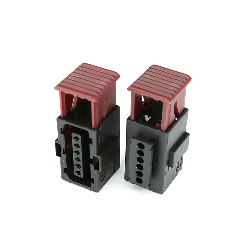
Surface-mount PCB Connector parts depend on solder tail coplanarity to form a reliable joint during reflow, since a tail sitting even a few hundredths of a millimeter out of plane can produce a cold joint that passes visual inspection but fails under thermal cycling. Stamping tolerance on the connector's frame determines baseline coplanarity, but handling during tape-and-reel packaging and shipment can introduce additional deviation before the part ever reaches a pick-and-place machine. Factories producing high-volume PCB Connector components typically run coplanarity checks using laser measurement rather than visual inspection alone, since the tolerance window relevant to reflow soldering is smaller than what the human eye reliably catches.
Retention Force And Mating Cycle Testing
Buyers sourcing connectors for applications involving repeated disconnection typically request test data covering several mechanical factors before approving a supplier:
- Insertion and withdrawal force measured across the full rated cycle count
- Contact resistance drift after cyclic testing, compared against the initial baseline reading
- Housing latch retention force under vibration, relevant for automotive and industrial mounting
- Plating adhesion results after thermal shock cycling between temperature extremes
A PCB Connector rated for a given number of mating cycles should hold contact resistance within a defined tolerance band throughout that entire rated life, not only at the beginning, which is why cycle testing data matters more to procurement teams than a single cycle-count number printed on a datasheet.
Pitch Tolerance And Mold Precision
Connector pitch — the spacing between adjacent contacts — depends on mold cavity precision during the housing's injection molding stage, and even small mold wear over a long production run can shift pitch outside tolerance before an operator notices visually. A PCB Connector with pitch drift beyond a few hundredths of a millimeter risks misalignment when mated against a board footprint machined to the original specification, producing stress on the contact legs during mating rather than a clean, even engagement. Mold makers producing tooling for fine-pitch connector series, particularly those below 1.5mm spacing, typically build in scheduled cavity inspection intervals rather than relying on total shot count alone, since cavity wear rates vary with the specific resin and glass-fiber content used in the housing material.